
Volgens mij is je experiment geslaagd.Ik begrijp ook niet hoe het kan werken, waar zit de terugkoppeling in het circuit?
Wellicht is het maar een digitaal artefact...?

Install the app
How to install the app on iOS
Follow along with the video below to see how to install our site as a web app on your home screen.
Note: This feature may not be available in some browsers.
You are using an out of date browser. It may not display this or other websites correctly.
You should upgrade or use an alternative browser.
You should upgrade or use an alternative browser.
Storing-Synth
- Thread starter ProgHead
- Start date


- Lid sinds
- 12 oktober 2016
- Berichten
- 7.677
Misschien weet AI het wel hoe dat kan?
Heb het eerste circuit geupload naar ChatGPT en krijg dit:
Here’s what I found when inspecting the circuit diagram:
The Falstad circuit simulator is generally accurate for linear components (R, L, C, ideal op-amps, transistors with built-in models), but certain situations can lead to oscillation that is both possible in reality and more pronounced in simulation.
Whether the oscillation is “real” or a simulation artefact depends mainly on:
 Likely Causes of Real Oscillation
If the circuit includes any of these:
- Positive feedback loops (e.g., an op-amp wired with gain > 1 and some phase shift)
- High-gain amplifiers with insufficient compensation
- Resonant RLC networks where the damping is low
 Even small parasitic capacitances/inductances can trigger real oscillations.
 Falstad-Specific Artefacts
The simulator uses a time-step and numerical integration. Artefacts may appear when:
- Time step is too large → “ringing” or false oscillation
- Ideal components (perfect op-amps, switches, inductors) create unrealistic infinite bandwidth or no ESR
- Floating nodes or poorly defined initial conditions
These can create oscillations that wouldn’t be sustained in a real circuit. How to Tell the Difference
- Add small series resistances to capacitors/inductors (e.g., 0.1 Ω) → If oscillation stops, it was likely a numerical artefact.
- Reduce the simulation time step → If the oscillation changes dramatically, it’s probably simulation-related.
- Introduce real-world parasitics (op-amp bandwidth, resistor tolerance) → If it still oscillates, it’s physically plausible.
 Next Step
If you can describe the circuit (or share the component list and connections),
I can point to the specific feedback path or component that is likely causing the oscillation.
- Lid sinds
- 12 oktober 2016
- Berichten
- 7.677
Vervolg:
I inspected the SVG you pointed at and extracted the schematic geometry so we can pinpoint the feedback path that’s making the thing oscillate. Short answer up front:
This looks like a real oscillation (a deliberate positive-feedback/phase-shift loop), not just a Falstad numerical glitch.
Below I show what I found in the diagram, how the loop is formed, and the simple checks you can run in Falstad (and what to change) to prove whether it’s physical or a simulator artefact.
I parsed the SVG and located the major items and node coordinates (I’ll refer to approximate pixel coordinates from the SVG so you can find the same places visually):
I also reconstructed the important wiring (graph of nodes) so we can see the actual connections:
(If you open the SVG in a text editor or Falstad viewer, those positions will match the same parts of the drawing.)
From the geometry and labels the circuit contains the elements that produce intentional oscillation:
So the topology looks like a classical phase-shift or two-op-amp oscillator: phase shift network → amplifier → positive feedback that closes the loop with enough gain to sustain oscillation.
That makes the oscillation physically plausible — you would get a real oscillation in hardware unless the op-amps or components limit the gain or add damping.
Run these controlled tests in Falstad (or any transient circuit simulator / breadboard):
If after these the oscillation remains at roughly the same frequency and amplitude, it’s almost certainly a real design oscillation (i.e., you'd see it on a physical breadboard with the same parts and op-amps).
I inspected the SVG you pointed at and extracted the schematic geometry so we can pinpoint the feedback path that’s making the thing oscillate. Short answer up front:
This looks like a real oscillation (a deliberate positive-feedback/phase-shift loop), not just a Falstad numerical glitch.
Below I show what I found in the diagram, how the loop is formed, and the simple checks you can run in Falstad (and what to change) to prove whether it’s physical or a simulator artefact.
What I found in the schematic (from the SVG)
I parsed the SVG and located the major items and node coordinates (I’ll refer to approximate pixel coordinates from the SVG so you can find the same places visually):
- Two op-amp triangles:
- Op-amp 1 inputs at ≈ (118,176) - and (118,240) +. Output at ≈ (170,20
 .
. - Op-amp 2 inputs at ≈ (302,192) - and (302,256) +. Output at ≈ (354,224).
- Op-amp 1 inputs at ≈ (118,176) - and (118,240) +. Output at ≈ (170,20
- Resistors / labels:
- “1k” label near ≈ (226,19 — a resistor in the path between the two op-amps (i.e. from op-amp1 output toward the network that goes to op-amp2).
- “1M” label near ≈ (320,166) — a large feedback resistor (near op-amp2).
- “1k” label near ≈ (226,19
- Capacitor:
- “10µF” label near ≈ (30,262) — a capacitor on the left side (likely part of a coupling / timing network).
- Output labelled “Audio Out” at ≈ (464,240) — taken from op-amp2 output or its node.
I also reconstructed the important wiring (graph of nodes) so we can see the actual connections:
- Op-amp1 output (170,20 → short wire → series resistor region (192 → 216 → 248 px region) labeled 1k → continues to the network feeding op-amp2 inputs (node ≈ 272→302 px).
- Op-amp2 output (354,224) is the final audio output; a 1M resistor provides significant feedback (near op-amp2 top input region).
(If you open the SVG in a text editor or Falstad viewer, those positions will match the same parts of the drawing.)
Why it oscillates (circuit explanation)
From the geometry and labels the circuit contains the elements that produce intentional oscillation:
- A multi-stage amplifier chain — two op-amps in series. Op-amp1 drives the network, op-amp2 amplifies and feeds back to earlier stage(s).
- A frequency-selective network (R/C) between stages. The 10µF and the resistor chain form a network that will have a frequency where the overall loop phase shift around the loop is ~0° (360°) and the loop gain ≥ 1 — the Barkhausen condition for sustained oscillation.
- A high value feedback resistor (1 MΩ) around op-amp2 gives the loop enough DC/low-freq gain so the net loop gain at the design frequency exceeds unity.
- The label “40 kHz” on the SVG suggests the circuit was designed to oscillate near 40 kHz — consistent with an RC network + op-amp gain tuned to that frequency.
So the topology looks like a classical phase-shift or two-op-amp oscillator: phase shift network → amplifier → positive feedback that closes the loop with enough gain to sustain oscillation.
That makes the oscillation physically plausible — you would get a real oscillation in hardware unless the op-amps or components limit the gain or add damping.
How to tell whether it’s simulator artefact vs real (quick tests)
Run these controlled tests in Falstad (or any transient circuit simulator / breadboard):
- Add small real-world damping
- Put a small series resistor with each capacitor (e.g. 1–100 Ω) or add a small series resistor to inductors (if any).
- Add a 1 MΩ → 10 MΩ bleed resistor from floating nodes to ground if nodes are floating.
- If the oscillation disappears immediately or dramatically changes, it was likely sensitive and possibly a numerical artefact or an unrealistic ideal-component behavior. If it persists, it’s likely real.
- Limit op-amp bandwidth
- Falstad often uses ideal op-amps by default (infinite bandwidth). Replace the ideal op-amp with a model that has finite open-loop gain/bandwidth (or insert a dominant-pole small capacitor across the op-amp’s feedback to emulate GBW).
- If the oscillator vanishes when you impose a realistic GBW limit, the simulated oscillation relied on unrealistic infinite bandwidth.
- Refine the simulator timestep
- Reduce the time step (increase accuracy) and re-run.
- If oscillation frequency or amplitude changes drastically with timestep, that’s a sign of numerical artifact. If it stays the same, it’s more likely physical.
- Start with zero initial condition vs. small perturbation
- Real oscillators need a perturbation to start (noise, initial condition). In simulation sometimes the solver’s numerical rounding provides that kick. If you force zero initial condition and the simulator never starts oscillating unless you give a tiny transient “kick” (voltage source brief pulse), it behaves like a real oscillator (needs startup energy). If it spontaneously starts from perfect zero and is unaffected by changing initial conditions, that’s suspicious.
- Add realistic component parasitics
- Add small ESR to capacitors, finite output impedance for sources, and finite open-loop gain to op-amps. Real circuits have these. If oscillation is robust to realistic parasitics, it will occur in hardware.
- Try a SPICE model
- If possible, rebuild the circuit in a SPICE engine (e.g. ngspice) with real op-amp models. SPICE’s device models and numerical methods are generally more realistic for analog oscillators; agreement strengthens the “real” verdict.
Practical quick changes you can do right now in Falstad (recommended)
- Insert a 10–100 Ω series resistor in series with the 10µF (and other capacitors). Re-run.
- Insert a 10 kΩ or 100 kΩ resistor from any floating node to ground.
- Replace the ideal op-amps with a lower-gain model or limit GBW (if Falstad has an op-amp element with gain/bandwidth settings).
- Reduce the simulator step size / increase accuracy in Falstad’s Options → Simulation step (or equivalent menu).
- Add a tiny voltage transient (pulse) to see if the oscillator needs a kick to start.
If after these the oscillation remains at roughly the same frequency and amplitude, it’s almost certainly a real design oscillation (i.e., you'd see it on a physical breadboard with the same parts and op-amps).
Summary (concise)
- The SVG wiring shows a closed loop: op-amp1 → RC network → op-amp2 → feedback (1 MΩ) → earlier node. That’s exactly the structure that produces sustained oscillation when loop phase/gain conditions are met.
- Because the topology and component values (10 µF, 1 kΩ, 1 MΩ, labeled 40 kHz) match a designed oscillator, the oscillation is very likely real and not only a Falstad numerical artefact.
- Still run the practical tests above (small series resistances, limit op-amp bandwidth, change timestep, and/or simulate in SPICE) to confirm; if it survives those changes, it will survive in hardware.
Practical quick changes you can do right now in Falstad (recommended)
- Insert a 10–100 Ω series resistor in series with the 10µF (and other capacitors). Re-run.
- Insert a 10 kΩ or 100 kΩ resistor from any floating node to ground.
- Replace the ideal op-amps with a lower-gain model or limit GBW (if Falstad has an op-amp element with gain/bandwidth settings).
- Reduce the simulator step size / increase accuracy in Falstad’s Options → Simulation step (or equivalent menu).
- Add a tiny voltage transient (pulse) to see if the oscillator needs a kick to start.
If after these the oscillation remains at roughly the same frequency and amplitude, it’s almost certainly a real design oscillation (i.e., you'd see it on a physical breadboard with the same parts and op-amps).
Het tweede punt doet de oscillatie teniet.
- Lid sinds
- 12 oktober 2016
- Berichten
- 7.677
Echt heel superbruikbaar lijkt me het trouwens niet als je kijkt naar de audio.
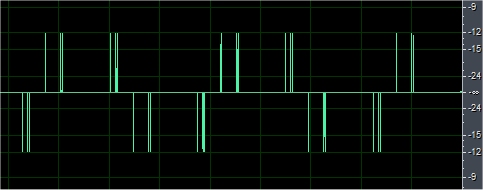
Uitvergroot, pulsjes van één enkele sample:
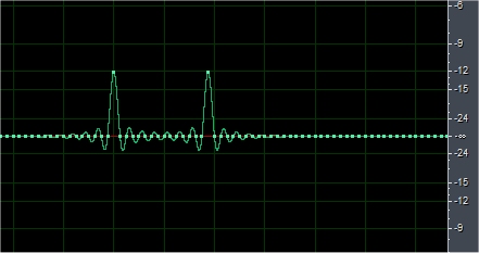
Uitvergroot, pulsjes van één enkele sample:
Voor House muziek wellicht, of Techno...  Niet mijn kopje thee, maar de lol van dit project zit hem er voor mij niet in om er muziek mee te maken (dat laat ik aan anderen over), maar om exotische circuits en ontwerpen te bedenken en uit te proberen. Wat je hier zou kunnen doen is er een extreme tijdsrek op toe te passen en er dan kicks e.d. mee aan te sturen of om de pulsjes als control signals te gebruiken om andere synths mee aan te sturen. Nog een andere optie is om de pulsjes te tellen, en dan steeds na een groot aantal van X pulsjes een puls door te laten zodat je het ook realtime kunt gebruiken.
Niet mijn kopje thee, maar de lol van dit project zit hem er voor mij niet in om er muziek mee te maken (dat laat ik aan anderen over), maar om exotische circuits en ontwerpen te bedenken en uit te proberen. Wat je hier zou kunnen doen is er een extreme tijdsrek op toe te passen en er dan kicks e.d. mee aan te sturen of om de pulsjes als control signals te gebruiken om andere synths mee aan te sturen. Nog een andere optie is om de pulsjes te tellen, en dan steeds na een groot aantal van X pulsjes een puls door te laten zodat je het ook realtime kunt gebruiken.
- Lid sinds
- 12 oktober 2016
- Berichten
- 7.677
Ah, okay. Maar ik dacht dat je op zoek was naar iets dat rechtstreeks geluiden kan produceren.
Ah, okay. Maar ik dacht dat je op zoek was naar iets dat rechtstreeks geluiden kan produceren.
Dat zou nog mooier zijn. Maar het een sluit het ander niet uit. Als dit idee werkt als een soort chaotische Rhythm Box met standaard geluidjes, dan zal het ook werken als aansturing/modulator van echte storingsbronnen. Het wordt daarbij dan slechts een "module" binnen het gehele circuit van de storing-synth.
Hover
-
Geen idee of een Demon box misschien kan helpen. Werkt op basis van electromagnetische velden (EMF)

 eternalresearch.com
The Demon Box
Eternal Research creates instruments that reveal hidden music in everyday objects. Using EMF detection and proprietary inductors, the Demon Box transforms electromagnetic fields from devices like phones and TVs into raw, sculptable soundscapes.
Daar moet ik voor inschrijven om het te bekijken. Maar Nap heeft mij ook al op dat toestel gewezen. Een van de opties voor mijn storing-synth is inderdaad het oppikken van elektromagnetische velden wat kan met antennes, spoelen of gevoelige condensator platen. Daar ga ik later nog mee experimenteren om dat in het circuit op te nemen.


Oh bedoel je dat! In deze fase van dit project ben ik enkel bezig met het uitproberen van principes. Dus die potmeter zal later door een ander storingsgestuurd circuit vervangen moeten worden. Wat deze simulatie laat zien is hoe je het signaal van een ruisbron kunt omvormen in een reeks random "tikken" (dat wil zeggen in een random ritme) met een moduleerbare gemiddelde frequentie.
- Lid sinds
- 12 oktober 2016
- Berichten
- 7.677
Het begint al aardig gestoord te klinken...

Nou het is je zeker gelukt om storing te synthetiseren!
Wat is dit voor building block?
Dat is een ruisbron, in hardware kun je daarvoor in de plaats bijvoorbeeld de thermische ruis van een weerstand gebruiken en die dan extreem versterken. Ik weet niet hoe je dat simuleert. Moet ik nog uitzoeken, of misschien weet iemand hier dat al?
Vergelijkbare discussies

- Reacties
- 15
- Bekeken
- 893


- Reacties
- 30
- Bekeken
- 2K

- Reacties
- 11
- Bekeken
- 921


- Reacties
- 7
- Bekeken
- 742

- Reacties
- 32
- Bekeken
- 2K

Delen: